Contact us

- Contact number:0755-2708-8292
- Mobile Number:18938693455(Helen Yu)
- Enterprise Email:yw11@zldsmt.com
- Shenzhen Factory (Headquarters):Building A3, Huafa Industrial Park, Fuyong Street, Fuyuan Road, Baoan District, Shenzhen
- Nantong Factory Address:No.268 Jinchuan Road, Nantong Hi-tech Industrial Development Zone, Tongzhou District, Nantong City, Jiangsu Province
- Kunshan Factory Address:No.1318, Shuixiu Road, North Private Industrial Park, Yushan Town, Kunshan City, Jiangsu Province

Precision micro-hole etching process
- 1. Medical Devices: For microfluidic chips and precision drug delivery components. 2. Electronic Components: For micro-vias in PCBs and semiconductor packaging parts.
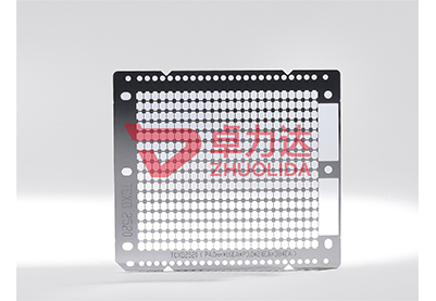
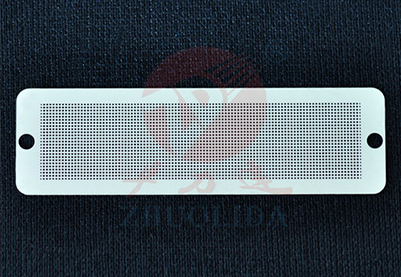
Precision micro-hole etching process adopts advanced photochemical etching technology, tailored to the core requirements of micro-hole manufacturing—ultra-precision, uniformity, and structural integrity. This process integrates micro-level control, material compatibility, and batch consistency, making it the optimal solution for high-performance micro-holes used in medical and electronic fields, where precision directly determines product functionality.
First, the etching process achieves exceptional dimensional precision, the core advantage of precision micro-hole manufacturing. The etching tolerance can reach ±0.001mm, with micro-hole diameters controllable between 0.05mm and 0.5mm, ensuring consistent size across every hole. Unlike mechanical drilling or laser drilling, chemical etching is a non-contact, cold process that avoids thermal damage, burrs, and hole tapering, ensuring each micro-hole is perfectly round, smooth-walled, and dimensionally stable.
Second, the etching process ensures superior uniformity and surface quality. The automated etching system precisely controls etchant concentration, temperature, and processing time, achieving uniform hole distribution and consistent depth. The smooth, burr-free hole surface (Ra ≤ 0.10μm) prevents particle accumulation, reduces friction, and avoids material deformation, which is critical for microfluidic flow in medical devices and signal transmission in electronic components.
Third, the etching process offers strong batch stability and process flexibility. It ensures consistent quality across large production runs, with a yield of over 99.7%, minimizing waste and rework. The process supports various micro-hole patterns—including single holes, dense arrays, and custom configurations—tailored to the specific needs of medical and electronic applications, without the need for expensive tooling adjustments.
Show picture


Precision micro-hole etching process via photochemical etching has distinct advantages over traditional mechanical drilling, laser cutting, and electroforming processes, especially for optimizing micro-hole precision and uniformity. Its application fields focus on medical devices and electronic components—two fast-growing industries driven by miniaturization and high-performance requirements—making it an indispensable technology for modern manufacturing.
In terms of etching advantages, first, it solves the core challenge of producing high-precision micro-holes without material damage. Mechanical drilling at the micro-scale often causes burrs, cracked edges, and inconsistent sizes due to tool wear and vibration, while laser drilling generates heat that creates a recast layer and thermal stress, degrading material properties. Etching avoids these issues, delivering pristine, stress-free micro-holes with consistent dimensions and smooth surfaces.
Second, it offers superior cost efficiency and design flexibility. Unlike electroforming, which requires expensive custom molds and long lead times, etching eliminates hard tooling needs—design modifications only require updating the photomask, reducing custom development costs by over 85%. For large-volume production, the automated line ensures high throughput and low per-unit costs, suitable for both premium medical devices and high-volume electronic components.
Third, it has strong material adaptability. The process can etch micro-holes in a wide range of materials, including stainless steel, copper, titanium, and PC, while preserving their inherent properties—such as biocompatibility for medical use and conductivity for electronic components. This versatility makes it suitable for diverse micro-hole applications, from medical microfluidics to electronic micro-vias.
In terms of industry applications, the first major field is medical devices. Etched precision micro-holes are critical for microfluidic chips, enabling precise control of fluid flow for diagnostic tests and drug delivery. They are also used in surgical instruments and medical sensors, where their smooth surface and biocompatibility prevent bacterial adhesion and tissue irritation, meeting strict healthcare safety standards.