Contact us

- Contact number:0755-2708-8292
- Mobile Number:18938693455(Helen Yu)
- Enterprise Email:yw11@zldsmt.com
- Shenzhen Factory (Headquarters):Building A3, Huafa Industrial Park, Fuyong Street, Fuyuan Road, Baoan District, Shenzhen
- Nantong Factory Address:No.268 Jinchuan Road, Nantong Hi-tech Industrial Development Zone, Tongzhou District, Nantong City, Jiangsu Province
- Kunshan Factory Address:No.1318, Shuixiu Road, North Private Industrial Park, Yushan Town, Kunshan City, Jiangsu Province
Ceramic Laminates Processing
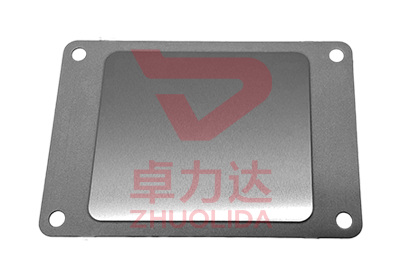
- 1. Electronic Devices: For insulating substrates in circuit boards and semiconductors. 2. Industrial Equipment: For high-temperature insulation components in machinery. 3. Architectural Decoration: For durable
- aesthetic ceramic laminate panels.


Ceramic Laminates Processing adopts advanced photochemical etching technology, tailored to the unique properties of ceramic laminates—high hardness, excellent insulation, heat resistance, and corrosion resistance. This process integrates ultra-precision, structural stability and material integrity, making it the optimal processing method for high-performance ceramic laminates used in diverse high-demand scenarios.
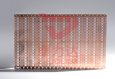
Second, the etching process ensures excellent surface quality and material performance retention. The etched ceramic laminate surface is smooth and burr-free, with a roughness Ra≤0.15μm, avoiding surface defects that could affect insulation performance or structural integrity. The process does not alter the ceramic’s inherent properties, maintaining its high hardness (Mohs 6-8), heat resistance (up to 1200°C), and electrical insulation, which are essential for long-term stable operation in harsh environments.
Third, the etching process offers strong batch stability and process flexibility. The automated etching system precisely controls etchant concentration, temperature, and processing time, ensuring consistent dimension, surface quality, and performance across every ceramic laminate in a production run, with a yield of over 99.5%. It supports etching of complex patterns—including micro-holes, precision slots, and custom designs—customized to the specific requirements of electronic, industrial and architectural applications.
Ceramic Laminates Processing via photochemical etching has distinct advantages over traditional mechanical cutting, laser cutting, and grinding processes, especially for handling the brittle nature and precision requirements of ceramic laminates. Its application fields cover electronic devices, industrial equipment, and architectural decoration—industries that demand high-performance, durable, and precise components—with broad market prospects driven by the development of high-tech and construction industries.
In terms of etching advantages, first, it solves the core challenge of processing brittle ceramic laminates without damage. Unlike mechanical grinding, which often causes chipping, cracking, or uneven surfaces, etching is a non-contact process that eliminates mechanical stress, ensuring the laminate’s flatness and structural integrity. Laser cutting, by contrast, generates high heat that can melt or deform ceramic materials, causing surface damage and reducing performance—issues that etching completely avoids.
Second, it offers superior precision and cost efficiency. The etching process achieves micro-level precision that is difficult to replicate with traditional methods, making it ideal for precision electronic substrates and industrial insulation components. It eliminates the need for expensive molds required for stamping, reducing initial investment by more than 80%. For large-volume production, the automated line improves efficiency and reduces labor costs, while the closed-loop etchant system minimizes waste and operational costs.
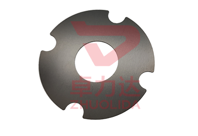
Third, it has strong flexibility and adaptability. The process can be customized to adjust ceramic laminate thickness (0.05mm-2.0mm), dimension, and pattern according to specific application needs—whether for micro-insulating substrates in electronics, high-temperature components in industrial machinery, or decorative panels in architecture. It also supports post-processing treatments—such as polishing and anti-corrosion coating—to further enhance surface performance and durability, expanding its application scope.
In terms of industry applications, the first major field is electronic devices, where etched ceramic laminates are used for circuit board substrates, semiconductor insulators, and electronic sensor components—relying on their excellent insulation and precision to ensure stable electronic performance. The second field is industrial equipment, where they serve as high-temperature insulation components, machine casings, and wear-resistant parts, leveraging their heat resistance and durability.
Customer we are doing our best to provide our bestservices to our customers with competitivetech solutions and high quality products,Zhuolida has won wide recognition from ourcustomers in all kinds of industry, andthis have laid a solid foundation for Zhuolida to be an leading brand in etchingindustry in China and a reputablemanufacturer |  |
 | Technology Zhuolida is an etching factory in China with varietiesof process, our company process techniques includechemical etching, laser cutting, EDM, stampingelectroforming, electroplating, electrophoresis. |
Enviroment We have self-built sewage treatment system,the wastewater reuse rate reaches 40% |  |