Contact us

- Contact number:0755-2708-8292
- Mobile Number:18938693455(Helen Yu)
- Enterprise Email:yw11@zldsmt.com
- Shenzhen Factory (Headquarters):Building A3, Huafa Industrial Park, Fuyong Street, Fuyuan Road, Baoan District, Shenzhen
- Nantong Factory Address:No.268 Jinchuan Road, Nantong Hi-tech Industrial Development Zone, Tongzhou District, Nantong City, Jiangsu Province
- Kunshan Factory Address:No.1318, Shuixiu Road, North Private Industrial Park, Yushan Town, Kunshan City, Jiangsu Province
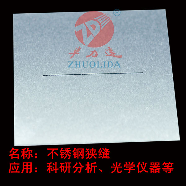
0.03mm slit plate processing
- 1. Optical Equipment: For light filtering and beam shaping in optics. 2. Semiconductor: For precision slits in semiconductor testing equipment. 3. Medical Devices: For sample separation in medical diagnostic instruments.

0.03mm slit plate processing adopts advanced photochemical etching technology, specifically tailored for ultra-thin slit plates with 0.03mm thickness—focusing on micro-level precision, structural stability and uniform slit performance. This process integrates ultra-fine slit control, material integrity and batch consistency, making it the optimal processing method for high-performance 0.03mm slit plates used in precision equipment.
First, the etching process achieves ultra-high precision for 0.03mm ultra-thin slit plates, critical for their application in precision scenarios. The etching tolerance can reach ±0.001mm, with slit width controllable between 0.01mm and 0.1mm, and slit straightness error within 0.002mm per 100mm. Unlike mechanical cutting or stamping, chemical etching is a non-contact, cold process that avoids thermal deformation and mechanical stress—key for ultra-thin 0.03mm plates, which are prone to bending or damage during traditional processing.
Second, the etching process ensures excellent surface quality and structural integrity. The etched 0.03mm slit plate surface is smooth and burr-free, with a roughness Ra≤0.1μm, avoiding surface defects that could affect light transmission, sample passing or signal accuracy. The process does not alter the base material’s (stainless steel, beryllium copper) chemical composition, maintaining its corrosion resistance and mechanical strength, ensuring the ultra-thin slit plate remains stable and durable in long-term use.
Third, the etching process offers strong batch stability and process flexibility. The automated etching system precisely controls etchant concentration, temperature, and processing time, ensuring consistent 0.03mm thickness, slit width, and surface quality across every slit plate in a production run, with a yield of over 99.7%. It supports processing of various slit shapes—including straight slits, curved slits, and multi-slit arrays—customized to the precision requirements of optical, semiconductor and medical equipment.
0.03mm slit plate processing via photochemical etching has distinct advantages over traditional mechanical cutting, laser cutting, and wire cutting processes, especially for handling the ultra-thin 0.03mm thickness and micro-slit precision. Its application fields cover optical equipment, semiconductor, and medical devices—industries that demand ultra-precision, ultra-thin slit components—with broad market prospects driven by the development of precision manufacturing and high-tech equipment.
In terms of etching advantages, first, it solves the core challenge of processing ultra-thin 0.03mm slit plates without damage. Unlike mechanical stamping, which often causes bending, deformation or slit edge burrs in ultra-thin plates, etching is a non-contact process that eliminates mechanical stress, ensuring the slit plate’s flatness and structural integrity. Laser cutting, by contrast, generates high heat that can melt the ultra-thin material, causing slit edge deformation and affecting precision—issues that etching completely avoids.
Second, it offers superior precision and cost efficiency for micro-slit production. The etching process achieves micro-level slit control that is difficult to replicate with traditional methods, making it ideal for 0.03mm ultra-thin slit plates used in optical beam shaping and semiconductor testing. It eliminates the need for expensive molds required for stamping, reducing initial investment by more than 80%. For large-volume production, the automated line improves efficiency and reduces labor costs, while the closed-loop etchant system minimizes waste and operational costs.
Third, it has strong flexibility and adaptability. The process can be customized to adjust 0.03mm slit plate thickness (with slight variations), slit width, and slit arrangement according to specific application needs—whether for single micro-slits in optical equipment, multi-slit arrays in semiconductors, or precision slits in medical diagnostic instruments. It also supports post-processing treatments—such as polishing and passivation—to further enhance surface smoothness and corrosion resistance, expanding its application scope.
In terms of industry applications, the first major field is optical equipment, where etched 0.03mm slit plates are used for light filtering, beam shaping, and optical sensing—relying on their precise slit width and smooth edges to ensure stable light transmission. The second field is semiconductor, where they serve as precision slits in semiconductor testing equipment, wafer inspection tools, and lithography machines, leveraging their ultra-precision to ensure accurate testing and manufacturing.
The third field is medical devices, where etched 0.03mm slit plates are used for sample separation, fluid control, and diagnostic sensing in medical instruments, requiring ultra-thin thickness and precise slits to meet strict medical standards. In addition, they are used in aerospace optics and precision measuring equipment, providing reliable ultra-thin slit solutions for high-performance devices. With the demand for ultra-precision, ultra-thin components growing in high-tech industries, 0.03mm slit plate processing will remain a critical technology for precision manufacturing advancement.
Customer we are doing our best to provide our bestservices to our customers with competitivetech solutions and high quality products,Zhuolida has won wide recognition from ourcustomers in all kinds of industry, andthis have laid a solid foundation for Zhuolida to be an leading brand in etchingindustry in China and a reputablemanufacturer |  |
 | Technology Zhuolida is an etching factory in China with varietiesof process, our company process techniques includechemical etching, laser cutting, EDM, stampingelectroforming, electroplating, electrophoresis. |
Enviroment We have self-built sewage treatment system,the wastewater reuse rate reaches 40% |  |