Contact us

- Contact number:0755-2708-8292
- Mobile Number:18938693455(Helen Yu)
- Enterprise Email:yw11@zldsmt.com
- Shenzhen Factory (Headquarters):Building A3, Huafa Industrial Park, Fuyong Street, Fuyuan Road, Baoan District, Shenzhen
- Nantong Factory Address:No.268 Jinchuan Road, Nantong Hi-tech Industrial Development Zone, Tongzhou District, Nantong City, Jiangsu Province
- Kunshan Factory Address:No.1318, Shuixiu Road, North Private Industrial Park, Yushan Town, Kunshan City, Jiangsu Province
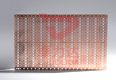
Semiconductor Kovar Alloy Cover Plate
- Semiconductor packaging
- integrated circuit (IC) hermetic sealing
- hybrid circuit casings
- semiconductor sensors
- aerospace and defense electronic components
- optical communication devices
- medical electronic equipment
- and high-reliability electroni
The Semiconductor Kovar Alloy Cover Plate adopts advanced photochemical etching technology, which is the optimal processing method for Kovar alloy due to its non-contact and high-precision advantages, making it widely recognized in the semiconductor packaging industry. Kovar alloy itself is a nickel-iron-cobalt controlled expansion alloy, and its etching characteristics are closely combined with the material’s inherent properties to ensure the product’s performance and applicability.
First, the etching process achieves ultra-high precision control, which is crucial for semiconductor components requiring strict size accuracy. The etching precision can reach ±0.005mm, and the aperture can be controlled between 0.01mm and 0.5mm, fully meeting the requirements of high-density integrated circuits for micro-structures. Unlike traditional mechanical processing, chemical etching uses a chemical solution to dissolve materials, avoiding mechanical stress and deformation, ensuring that the Kovar alloy’s low coefficient of thermal expansion (CTE) is not damaged, and maintaining its consistent expansion rate with glass and ceramics.
Second, the etching process ensures excellent surface quality and structural integrity. After etching, the surface of the cover plate is smooth and flat with a roughness Ra≤0.2μm, no burrs or scratches, and no need for secondary polishing, which can effectively reduce dust adhesion and improve the hermetic sealing performance of semiconductor packaging. At the same time, the etching process supports the molding of complex structures, including micro holes, elliptical holes, sine wave gratings, step structures, and special-shaped slots, which can be customized according to the design requirements of different semiconductor devices.
Third, the etching process has excellent batch stability and compatibility. The roll-to-roll etching production line can stably achieve high-yield mass production, with a product yield of over 99.2%, which is far higher than traditional stamping processes. The process is compatible with various thicknesses of Kovar alloy substrates (0.01mm to 1.0mm), solving the problem of easy breakage of ultra-thin materials in traditional processing. In addition, the etching process can be combined with PVD coating, passivation, and other surface treatment processes to further enhance the product’s corrosion resistance and service life.
The Semiconductor Kovar Alloy Cover Plate, processed by photochemical etching, has significant advantages over traditional processing methods such as stamping and laser cutting, and its application fields cover multiple high-end industries that require high precision and high reliability, especially in the semiconductor and aerospace fields, showing broad market prospects.
In terms of etching advantages, first of all, it has obvious cost advantages and rapid iteration capabilities. Compared with the stamping process that requires tens of thousands of yuan in mold opening costs, the etching process only needs to make photomasks, reducing the mold opening cost by more than 80%. For small-batch trial production (≥10 pieces), rapid proofing can be realized within 24 hours, and the research and development cycle is shortened to 1/5 of the traditional process, helping enterprises save research and development costs and seize market opportunities.
Secondly, the etching process maintains the material properties to the greatest extent. Since the etching process is non-contact processing, it does not cause mechanical stress, deformation, or material fatigue to the Kovar alloy, ensuring that the alloy’s mechanical strength (yield strength ≥400MPa, elongation ≥15%) and thermal expansion performance remain intact, which is crucial for the long-term reliability of semiconductor packaging components. At the same time, the etched product has no burrs, avoiding short circuits caused by burrs in semiconductor devices.
Thirdly, the etching process has strong flexibility and customization capabilities. It can freely adjust the hole shape, aperture, and structure according to customer design requirements without replacing molds, which is suitable for the personalized needs of different semiconductor devices. Whether it is the micro-structure required for 5G communication modules or the special-shaped slots required for hybrid integrated circuits, the etching process can be accurately realized, providing customized solutions for various industries.
In terms of industry applications, the product is mainly used in the semiconductor industry, including semiconductor packaging, IC hermetic sealing, and semiconductor sensors. Its precise size and good hermetic sealing performance can effectively protect sensitive semiconductor components from moisture, dust, and other external factors, extending the service life of the devices. In the aerospace and defense industry, it is used in critical components such as thermocouples, connectors, and satellite interconnects, relying on its stable thermal and mechanical properties to withstand extreme temperatures and high-stress environments.
In addition, it is also widely used in medical electronic equipment and optical communication devices. In medical electronic equipment, the etched Kovar alloy cover plate has good biocompatibility and corrosion resistance, meeting the strict hygiene standards of the medical industry. In optical communication devices, its precise micro-structure can ensure the stability of signal transmission, improving the performance of the equipment. With the development of 5G, quantum computing, and other emerging technologies, the demand for high-precision semiconductor components will continue to grow, and the Semiconductor Kovar Alloy Cover Plate processed by etching will have broader application prospects.
Customer we are doing our best to provide our bestservices to our customers with competitivetech solutions and high quality products,Zhuolida has won wide recognition from ourcustomers in all kinds of industry, andthis have laid a solid foundation for Zhuolida to be an leading brand in etchingindustry in China and a reputablemanufacturer |  |
 | Technology Zhuolida is an etching factory in China with varietiesof process, our company process techniques includechemical etching, laser cutting, EDM, stampingelectroforming, electroplating, electrophoresis. |
Enviroment We have self-built sewage treatment system,the wastewater reuse rate reaches 40% |  |