Contact us

- Contact number:0755-2708-8292
- Mobile Number:18938693455(Helen Yu)
- Enterprise Email:yw11@zldsmt.com
- Shenzhen Factory (Headquarters):Building A3, Huafa Industrial Park, Fuyong Street, Fuyuan Road, Baoan District, Shenzhen
- Nantong Factory Address:No.268 Jinchuan Road, Nantong Hi-tech Industrial Development Zone, Tongzhou District, Nantong City, Jiangsu Province
- Kunshan Factory Address:No.1318, Shuixiu Road, North Private Industrial Park, Yushan Town, Kunshan City, Jiangsu Province

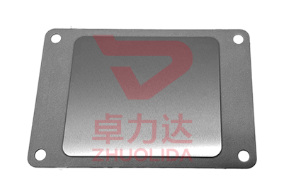
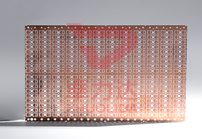
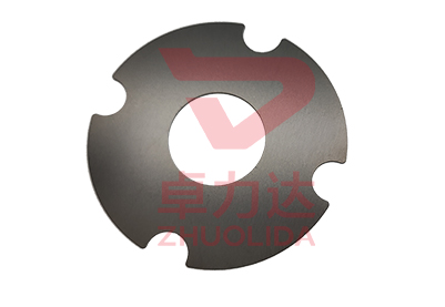
Grating Mask Plate Processing
- Optical Communication
- Spectroscopy Instruments
- Laser Systems
- Semiconductor Lithography
Grating Mask Plate Processing adopts state-of-the-art photochemical etching technology, a non-contact cold processing method that sets the gold standard for high-precision optical mask manufacturing. Unlike traditional mechanical engraving or laser ablation, chemical etching uses selective chemical corrosion to create ultra-precise grating structures on optical-grade substrates, enabling the production of grating masks with unmatched precision, optical clarity and durability—critical for applications where light diffraction, pattern transfer accuracy and transmission efficiency are non-negotiable.
The core advantage of etching in grating mask plate processing is its nanometer-level precision and grating uniformity. Etching technology achieves exceptional dimensional control, with grating line width error strictly controlled within ±0.0005mm, spacing deviation less than 0.0003mm, and groove depth uniformity within 0.001mm. This level of precision is essential for grating masks, as even minute variations in grating structure can disrupt light diffraction, reduce alignment accuracy and degrade optical performance. The etched grating masks feature perfectly uniform line patterns, smooth edges and consistent substrate thickness, ensuring optimal light dispersion, coupling and focusing in high-end optical systems.
Furthermore, etching ensures superior optical surface quality and light compatibility. As a cold processing method, it avoids the thermal damage, surface roughness and edge burrs associated with laser ablation or mechanical grinding—defects that cause light scattering, increase transmission loss and compromise optical clarity. Grating masks are typically made of high-purity optical-grade substrates (quartz, glass, silicon), and etching preserves their intrinsic optical properties, such as high transmittance, low refractive index variation and excellent thermal stability. The non-contact process eliminates surface scratches and microcracks, achieving an ultra-smooth surface (Ra≤0.008μm) that minimizes light loss and ensures stable optical performance in diverse working environments.
Show picture


Grating Mask Plate Processing using etching technology offers distinct competitive advantages over traditional manufacturing methods such as mechanical engraving, laser ablation and photolithographic stamping. These advantages make etched grating mask plates the preferred choice for global optical, communication and semiconductor manufacturers, where precision, optical performance and reliability are critical for product quality and functionality.
The primary advantage of etching in grating mask plate processing is its ability to produce ultra-precise, low-loss grating structures at scale. Laser ablation often causes thermal damage to substrate surfaces, resulting in rough groove edges, uneven depth and increased light scattering—issues that degrade optical clarity and transmission efficiency. Mechanical engraving is limited by tool precision, unable to achieve nanometer-level grating accuracy and consistent groove profiles. In contrast, etching produces grating masks with nanometer-level precision, smooth burr-free grooves and uniform surface quality, ensuring optimal light diffraction, focusing and transmission—critical for optical communication, spectroscopy and laser systems.
Another key benefit is optical performance preservation and cost-effectiveness. Etching is a non-damaging cold process that preserves the intrinsic optical properties of substrates, avoiding the light absorption and transmittance loss caused by thermal processing. Unlike traditional methods that require multiple post-processing steps (polishing, deburring, surface coating) to improve optical performance, etched grating masks are inherently smooth and defect-free, eliminating additional costs and production time. The non-contact process also reduces tool wear and maintenance costs, while high-volume production capabilities ensure consistent quality at a lower per-unit cost.
Etching also offers excellent substrate versatility and design flexibility. It supports a wide range of optical-grade substrates, including quartz (for high transmittance and thermal stability), glass (for cost-effectiveness) and silicon (for integrated optical applications). Additionally, etching can create complex grating patterns (such as blazed gratings, holographic gratings and gradient groove densities) that are difficult or impossible to achieve with traditional methods. This flexibility allows manufacturers to tailor grating masks to specific application needs, ensuring optimal performance in diverse optical scenarios.
Customer we are doing our best to provide our bestservices to our customers with competitivetech solutions and high quality products,Zhuolida has won wide recognition from ourcustomers in all kinds of industry, andthis have laid a solid foundation for Zhuolida to be an leading brand in etchingindustry in China and a reputablemanufacturer |  |
 | Technology Zhuolida is an etching factory in China with varietiesof process, our company process techniques includechemical etching, laser cutting, EDM, stampingelectroforming, electroplating, electrophoresis. |
Enviroment We have self-built sewage treatment system,the wastewater reuse rate reaches 40% |  |