Contact us

- Contact number:0755-2708-8292
- Mobile Number:18938693455(Helen Yu)
- Enterprise Email:yw11@zldsmt.com
- Shenzhen Factory (Headquarters):Building A3, Huafa Industrial Park, Fuyong Street, Fuyuan Road, Baoan District, Shenzhen
- Nantong Factory Address:No.268 Jinchuan Road, Nantong Hi-tech Industrial Development Zone, Tongzhou District, Nantong City, Jiangsu Province
- Kunshan Factory Address:No.1318, Shuixiu Road, North Private Industrial Park, Yushan Town, Kunshan City, Jiangsu Province
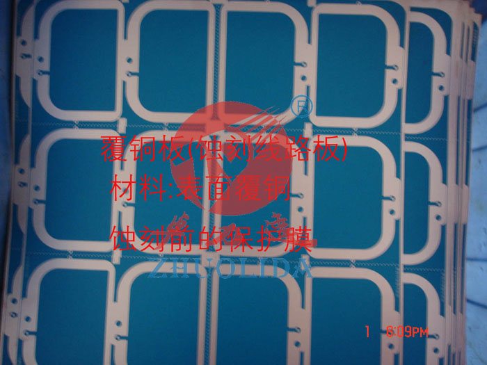
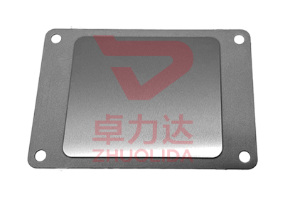
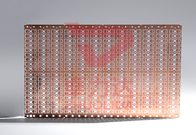
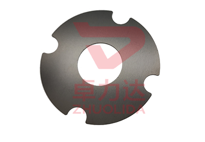
Copper-clad laminate etching
- 1. PCB Manufacturing: For circuit pattern etching in printed circuit boards of all types. 2. Electronic Devices: For conductive layers in smartphones
- computers and industrial control PCBs.
Copper-clad laminate etching adopts advanced photochemical etching technology, tailored to the core requirements of copper-clad laminates (CCL)—excellent conductivity, ultra-precise circuit pattern control, adhesion stability, and corrosion resistance. This process integrates micro-level precision control, copper-clad material compatibility, and batch consistency, making it the optimal manufacturing solution for high-performance CCL used in PCB and electronic device fields, where circuit precision directly determines electronic product reliability.
First, the etching process achieves exceptional circuit precision and pattern uniformity, the core of copper-clad laminate performance. The etching tolerance can reach ±0.001mm, with circuit line width, spacing, and copper layer thickness precisely controlled to meet strict PCB design standards. Unlike mechanical carving or laser etching, chemical etching is a non-contact, cold process that avoids thermal damage, edge burrs, and copper layer peeling, ensuring each circuit pattern is clear, uniform, and accurately positioned for stable signal transmission.
Second, the etching process preserves the inherent conductivity and adhesion of copper-clad laminates. The automated etching system precisely controls etchant concentration, temperature, and processing time, avoiding damage to the copper layer and substrate (FR-4, polyimide). The smooth, burr-free circuit surface (Ra ≤ 0.10μm) reduces signal loss and electromagnetic interference, while the intact copper-substrate adhesion ensures long-term stability, preventing copper layer detachment during PCB assembly and use.
Third, the etching process offers strong batch stability and design flexibility. It ensures consistent quality across large production runs, with a yield of over 99.7%, minimizing waste and rework—critical for mass-produced PCBs. The process supports various circuit patterns, including dense fine lines, complex layouts, and custom designs, tailored to the specific needs of consumer electronics and industrial control PCBs, without the need for expensive tooling adjustments.
Show picture

Copper-clad laminate etching via photochemical etching has distinct advantages over traditional mechanical carving, laser etching, and plasma etching processes, especially for optimizing circuit precision and copper layer stability. Its application fields focus on PCB manufacturing and electronic devices—two core sectors driven by the demand for miniaturized, high-performance electronic components—making it an indispensable technology for modern electronic manufacturing.
In terms of etching advantages, first, it solves the core challenge of producing fine, uniform circuit patterns on copper-clad laminates. Mechanical carving often causes uneven line widths, edge burrs, and copper layer damage, leading to signal interference and PCB failure. Laser etching generates heat that melts copper edges, altering conductivity and causing substrate deformation, affecting PCB performance. Etching avoids these issues, delivering precise, smooth circuit patterns with consistent copper layer thickness, ensuring stable signal transmission.
Second, it offers superior cost efficiency and design flexibility. Unlike traditional processing methods that require expensive tools for fine circuit etching, photochemical etching eliminates hard tooling needs—design modifications only require updating the photomask, reducing custom development costs by over 80%. For large-volume PCB production, the automated line ensures high throughput and low per-unit costs, suitable for both high-end precision PCBs and mass-produced consumer electronics PCBs.
Third, it has strong adaptability to different copper-clad laminate types. The process is tailored to handle various CCL materials, including FR-4, polyimide, and aluminum-based copper-clad laminates, while preserving their inherent properties—such as heat resistance for industrial PCBs and flexibility for flexible PCBs. It can etch copper layers of various thicknesses (0.01mm-0.1mm), maintaining consistent precision and surface quality, making it suitable for diverse PCB applications.
In terms of industry applications, the first major field is PCB manufacturing. Etched copper-clad laminates are the core of all printed circuit boards, used in single-layer, double-layer, and multi-layer PCBs for consumer electronics, industrial control, and aerospace. Their precise circuit patterns enable miniaturization of PCBs, meeting the demand for compact electronic devices, while their stable conductivity ensures reliable signal transmission.
Customer we are doing our best to provide our bestservices to our customers with competitivetech solutions and high quality products,Zhuolida has won wide recognition from ourcustomers in all kinds of industry, andthis have laid a solid foundation for Zhuolida to be an leading brand in etchingindustry in China and a reputablemanufacturer |  |
 | Technology Zhuolida is an etching factory in China with varietiesof process, our company process techniques includechemical etching, laser cutting, EDM, stampingelectroforming, electroplating, electrophoresis. |
Enviroment We have self-built sewage treatment system,the wastewater reuse rate reaches 40% |  |