


Contact us

- Contact number:0755-2708-8292
- Mobile Number:18938693455(Helen Yu)
- Enterprise Email:yw11@zldsmt.com
- Shenzhen Factory (Headquarters):Building A3, Huafa Industrial Park, Fuyong Street, Fuyuan Road, Baoan District, Shenzhen
- Nantong Factory Address:No.268 Jinchuan Road, Nantong Hi-tech Industrial Development Zone, Tongzhou District, Nantong City, Jiangsu Province
- Kunshan Factory Address:No.1318, Shuixiu Road, North Private Industrial Park, Yushan Town, Kunshan City, Jiangsu Province
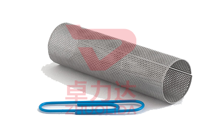
Roll-to-Roll Etching Processing
- 1. Semiconductor Industry: For micro-pattern processing of semiconductor wafers. 2. Flexible Electronics: For etching flexible circuit boards (FPC). 3. Solar PV: For patterning solar cell electrodes.
Roll-to-Roll Etching Processing is an advanced continuous photochemical etching technology, which is widely used in high-volume, high-precision electronic component manufacturing due to its unique processing characteristics and stable performance. Different from traditional sheet etching, it adopts a continuous roll feeding mode, which integrates cleaning, coating, exposure, etching, and stripping into one production line, realizing efficient and automated processing.
First, the etching process has excellent continuity and high efficiency. The roll-to-roll production line can realize 24-hour continuous operation, with a processing speed of 1-5m/min, which is 5-10 times higher than traditional sheet etching. This continuous processing mode greatly reduces manual operation, shortens the production cycle, and effectively improves production efficiency, which is especially suitable for mass production of electronic components such as FPC and solar cell electrodes.
Second, the etching precision is high and the processing quality is uniform. The roll-to-roll etching process adopts high-precision guide rail positioning and automatic tension control, which ensures that the substrate is flat and stable during the etching process, and the etching tolerance can reach ±0.005mm. At the same time, the uniform spray system ensures that the etching solution is evenly distributed on the substrate surface, avoiding uneven etching caused by local concentration differences, and the surface roughness of the etched product is Ra≤0.2μm.
Third, the process has strong compatibility and flexibility. It can process various roll-shaped substrates, including copper, aluminum, Kovar alloy, stainless steel, and other metal materials, as well as flexible materials such as PI and PET. The thickness of the processed substrate can be controlled between 0.01mm and 0.5mm, and it supports the etching of complex patterns such as micro holes, fine lines, and special-shaped structures. The pattern can be quickly adjusted by replacing the photomask, which is suitable for small-batch and multi-variety production.
Roll-to-Roll Etching Processing has obvious advantages over traditional sheet etching, laser cutting, and stamping processes, and its application fields are constantly expanding with the development of electronic information technology, covering semiconductor, flexible electronics, solar PV and other high-end industries, becoming an important support for the upgrading of the electronic manufacturing industry.
In terms of etching advantages, first of all, it has significant efficiency and cost advantages. The continuous production mode of roll-to-roll etching eliminates the need for manual feeding and unloading of sheet materials, reducing labor costs and improving production efficiency. The production capacity can reach 10,000 square meters per day, which is far higher than traditional sheet etching. At the same time, the closed-loop recycling of the etching solution reduces the cost of raw materials and waste liquid treatment, and the overall processing cost is reduced by 25%-35% compared with traditional processes.
Secondly, it maintains the integrity of the substrate performance. The roll-to-roll etching process is non-contact processing, which does not produce mechanical stress, deformation, or burrs on the substrate, ensuring that the mechanical properties, electrical conductivity, and thermal stability of the material are not damaged. This is crucial for sensitive electronic components such as semiconductor wafers and flexible circuit boards, which can effectively improve the reliability and service life of the products.
Thirdly, it has strong customization and scalability. The process can be flexibly adjusted according to the customer's needs, including substrate material, thickness, pattern design, and processing speed. The photomask replacement cycle is short (only 2-4 hours), which can quickly respond to the personalized needs of different customers and shorten the product research and development cycle. In addition, the production line can be expanded according to the production scale, realizing the flexible expansion of production capacity.
In terms of industry applications, the first major field is the semiconductor industry, which is used for the etching of semiconductor wafers, integrated circuit (IC) lead frames, and micro-sensors. Its high precision and stability ensure the performance of semiconductor components. The second field is flexible electronics, which is the core processing technology of flexible circuit boards (FPC), flexible displays, and wearable devices, realizing the etching of fine lines and complex patterns on flexible substrates.
