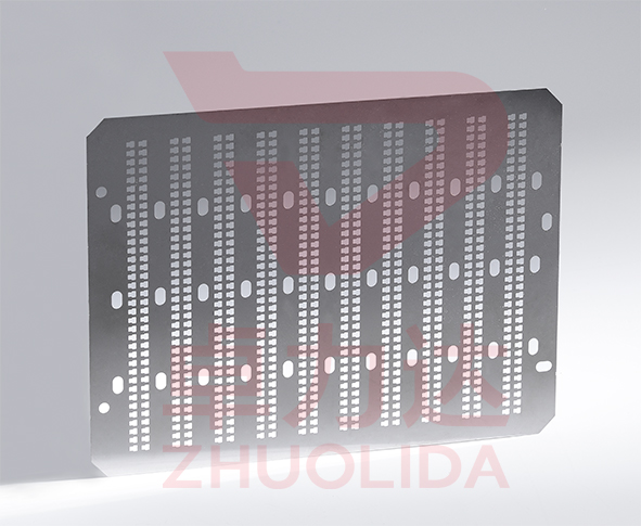
Recently, have you often come across the term "semiconductor lead frame"? So what is called semiconductor lead frame, lead frame is a key structural component with the help of bonding alloy wire to achieve the electrical link between the chip internal circuit lead end and the outer lead, forming an electrical circuit, its main role is to pass the IC chip signal to the outside world bridge, is also an important material for semiconductor back-end packaging. According to the function can be divided into power and discrete components, that is, mainly used to support diodes, light-emitting diodes, transistors and other products; integrated circuits used in the chip, printed circuit board media, with the function of conductivity. The vast majority of the semiconductor integrated blocks require the use of lead frames. Leadframe traditional packaging mainstream technology including SOT, SOP, QFN/DFN, etc., is a mature means of packaging and testing technology. Product types can be divided into TO, DIP, ZIP, SIP, SOP, SSOP, QFP (QFJ), SOD, SOT. raw materials are C194 copper, red copper, phosphor copper, KFC, 7025, TAMAC-15, PMC-90, etc.
The production process of semiconductor leadframes is mainly by die stamping method and chemical etching method, i.e. etching process,Semiconductor leadframe etching processThe chemical etching method can make the product burr-free, high precision, and defect-free product advantage.Semiconductor leadframe etching processMaterial thickness can be controlled at 0.05mm,0.08mm,0.09mm,0.1mm,0.15mm,0.2mm,0.3mm.


