


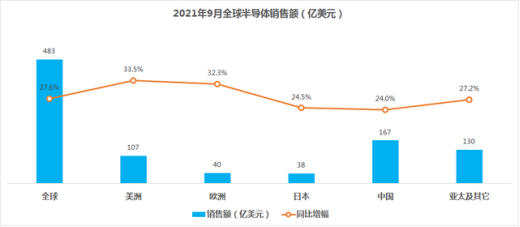
According to the Semiconductor Association of America (SIA) data, the global semiconductor market sales reached $ 391.54 billion in January-September 2021, up 23.14% year-on-year; China's semiconductor market sales reached $ 136.94 billion, up 24.76% year-on-year. From the perspective of each region of the world, China's semiconductor jumped to the world's largest market, sales accounted for 35%, mainly because of China's vast market, the demand for semiconductors itself is large; secondly, China's global electronics, home appliances and other manufacturing centers, the need to import integrated circuits to manufacture goods, and then sold to other parts of the world.
Semiconductor is a material with controllable electrical conductivity ranging from insulator to conductor. From the perspective of science and technology and economic development, semiconductors are used in integrated circuits, consumer electronics, communication systems, photovoltaic power generation, lighting, high-power power conversion and other fields, such as diodes using devices made of semiconductors. Semiconductors are divided into four categories: integrated circuits, discrete devices, sensors and optoelectronic devices, of which the integrated circuit market accounts for more than 80%. Integrated circuits (IC, commonly known as chips) are further divided into four main categories: memory (content), logic devices (CPU, GPU, etc.), microprocessors, and analog devices. Therefore, from the point of view of technology or economic development, the importance of semiconductors is very large, and daily life involves computers, cell phones or digital recorders among the core units have an extremely close relationship with semiconductors.
With the intensification of market competition, the manufacturing requirements of semiconductor processes are getting higher and higher, from 14mm development to 2mm threads, process development technology requirements continue to improve, the product component performance, efficiency, miniaturization requirements are extremely high. The traditional process stamping high cost, too hard, too small, fragile metal can not meet the requirements, on the edge of the cut to produce scratches, local burrs, very time-consuming also reveals the shortcomings of the process. The laser cutting disadvantages make the product produce scratches, burrs, etc., also can not meet the semiconductor high-precision, excellent quality characteristics.
Ltd. for the semiconductor industry to help the method, that is, photochemical etching, usually referred to as etching, through the etching process can achieve processing less than 0.1mm wall thickness of the plate to do structural processing, the process principle is through the plate exposure, after the development, the etched area of the protective film out, in the etching process so that the metal contact chemical solution, the use of two positive graphics through from both sides of the Chemical grinding to achieve the effect of dissolution corrosion, the formation of concave and hollow molding effect. Zhuolida etching process has a wealth of practical case experience, with the United States CHEMCUT etching line, Israel's light painting machine, France AUTOMA automatic roll-to-roll exposure machine and other advanced production equipment of internationally renowned brands, to provide a guarantee for the stability of semiconductor production, to import materials, mainly, to be able to etch different materials processing, thickness from 0.03mm-2.0mm; tolerance The minimum can be controlled in ± 0.01mm, can meet the semiconductor etching precision to tolerance micron level. Zollida etching process combines precision etching, electroplating, electrophoresis, anodic oxidation, precision electroforming, vacuum diffusion welding as a whole has been successfully practiced in semiconductor integrated circuit packaging with lead frames, semiconductor wafers, package inspection with contactors (spring terminals), probe cards / IC socket with test heads and guide plates, etc., but also for unmanned LIDAR communication coding ring, car stretch screen, folding screen, scroll We also provide specialized solutions for coding rings for unmanned LIDAR communication, in-vehicle stretch screens, folding screens, scroll screens, etc.
