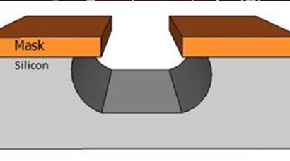
The semiconductor field often encounters tiny parts, and because of this it is necessary to proceed by way of micro-etching process, which is an extremely important step in the micro-manufacturing process. Etching refers to the removal of layers through the surface of the wafer when manufacturing, each wafer needs to undergo a lot of micro-etching process, and the material used to protect the wafer from etchant corrosion we call the mask material, the mask material can be photoresist, but also by photolithography for patterning. The etching process needs to control the etching time and etching rate through the cavity according to a specific depth. The removal of the top layer of a multilayer structure needs to be performed by an etcher without any kind of damage to the lower layer and the mask layer, mainly because it depends on the ratio of etch rates between the materials, i.e., selectivity. Etching weakens the mask layer and produces a cavity with an inclined sidewall called deviation.
The principle of wet etching in etching is the process of getting the material out of the wafer by means of a liquid chemical or etching solution. The mask can be limited to a specific pattern on the copper drum wafer to complete. The material not protected by the mask will be etched away by the etching solution. The mask deposited and framed on the lens can be executed by photolithography. The wet etching process involves multiple layers of chemical reactions that consume the original reactants to produce new reactants.


